Noise Measurement
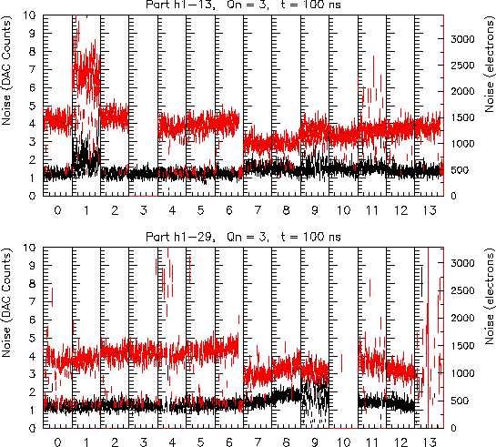
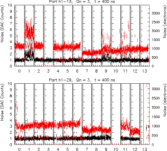
The results of the fitted noise values from the threshold scans
for all channels are summarized in the plots below.
The results are presented in units of
DAC counts (left side verical scale) and in SI units (right side vertical
scale). The chip numbers are also shown.
An average gain of 190 mV/fC was used for the conversion to SI units.
The gain measurements are discussed in the following section.
The data before bonding to the silicon are in black.
The data after bonding to the silicon are in red.
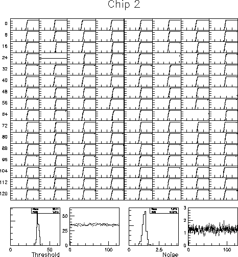
The full threshold scan data for the n-side charge injection value
of 3 are available in the links below. An example of the presentation
format for one chip is given below.
Before Bonding to the silicon:
- Threshold scan plots for H1-29, 100ns shaping
time, Qn=3.
- Threshold scan plots for H1-13, 100ns shaping
time, Qn=3.
- Threshold scan plots for H1-29, 400ns shaping
time, Qn=3.
- Threshold scan plots for H1-13, 400ns shaping
time, Qn=3.
After Bonding to the silicon:
- Threshold scan plots for H1-29 (D02F-4), 100ns shaping
time, Qn=3.
- Threshold scan plots for H1-13 (D02B-8), 100ns shaping
time, Qn=3.
- Threshold scan plots for H1-29 (D02F-4), 400ns shaping
time, Qn=3.
- Threshold scan plots for H1-13 (D02B-8), 400ns shaping
time, Qn=3.
Tables of the average noise for each chip at each charge injection
value can be found
here .
Average Noise Values
Qn=2, Qp=61

Qn=3, Qp=60

Qn=4, Qp=59

The conversion from counts to electrons above assumes an average gain
of 200 mV/fC before bonding to the silicon and 190 mV/fC after bonding
to the silicon. Chips 1 and 9 from
HDI H1-13 and
chips 9, 10, and 13
from HDI H1-29
were excluded from the averages due to abnormal behavior.
Some observations:
- For a shaping time of 100ns, the noise depends on how much charge is injected.
The average noise for three different charge injection values is shown
below.
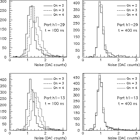
Before bonding to silicon.
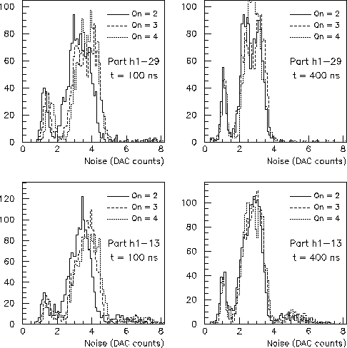
After bonding to silicon.
This effect was present in the data from the second h1 prototype
with version 1 of the rad-hard chip, although it was not as strong.
The effect was not present in the calibration data of the test
beam module (1st h1 prototype, V1 of rad-soft chip) taken at UCSB.
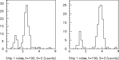
- The effect was much more prononced on chip 1 of DFA
D02F-4 (HDI H1-29).
For this chip
the noise as measured in a threshold scan with Q=2 was
much smaller than for Q=3 or 4. Interestingly enough,
for this chip the effect could also be seen with a shaping time
of 400 nsec. The noise on this chip for two runs with t=100 nsec
and Q=2 and 3 is shown below.
- Chip 9 shows an unusually high level of
coherent noise on both
H1-29
and H1-13.
This effect can be seen in the threshold scan
plots in the links above.
The effect was present in the tests of the second H1 prototype
with version 1 of the rad-hard chip. The effect was not
present in the calibration data for the test beam module which
were taken at UCSB. The test beam module used the first
H1 prototype and version 1 of the rad-soft chip. The effect
is either due to the UCSB test stand setup or a problem in the
H1 layout. The effect
appears for chip 9 on a forward and a backward HDI which isn't
in the same physical location on the HDI. This argues against the
hypothesis of an HDI layout problem.
Chip 9 is in the
same physical location in the ring frame test stand setup (the p-side
is always down), suggesting that perhaps this is effect is due to
some problem with the UCSB test-stand setup.
However, the effect persisted in the tests done
in the commissioning box, where the setup was quite different.
Therefore we think that it is highly unlikely that this problem
is due to peculiarities of the UCSB setup.
We also note that the gain
measurements for chip 9 are quite anomalous.
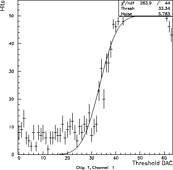
- Chip 1 on HDI H1-13 (DFA D02B-8)
had a digital problem that caused the threshold scan fits to give inflated noise values.
The plot below shows an example fit from chip 1.
After the data shown above were taken, the problem disappeared for
a while, but then a similar problem reappeared.
See the section on digital
problems for more details.
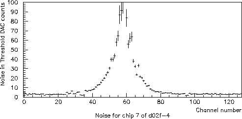
- After mounting the detector in the commissioning box, a region of
very high noise developed on chip 7 of DFA D02F-4
(HDI H1-29), see below.
The commissioning box was then opened, and the detector was carefully
inspected for signs of damage. No damage was found. Data was also taken
removing the aluminized mylar which is used as a shield for the
commissioning box and which is very close to the silicon and
the encapsulated bonds. The noise in the affected region
of chip 7 was still very high.
This problem is not understood.

Back to contents...
Forward to the next section...


![]()