HDI H1-29 (DFA D02F-4), chip 13. Read back tests of control registers and masks stopped working. The read back bits were typically the same as the written bits, but shifted by one position within the word.
Digital Problems
A number of digital problems were found in performing tests on the two hybrids. All tests were performed using CLOCK A only.
Before bonding to the siliconHDI H1-29, chip 13 is flaky. The trailer is a one followed by 15 zeros instead of 16 zeros. This chip is the rightmost chip on the p-side. Reading from the right does not always work. We believe that this is due to flakiness with the output from this chip. Therefore the p-side of this HDI should always be read from the left.
HDI H1-29, chip 10. The data/status bit on event data is sometime missing. The trigger tag is always zero (in the LBL ROM teststand setup the trigger tag should always be one). The trigger time is always zero.
HDI H1-29, chip 11. The trigger time is always zero.
HDI H1-13. Cannot read chips 2-3-4-5-6 from the left, see the visual inspection discussion. Therefore the n-side of this HDI should always be read from the right.
HDI H1-13, chip 0. After power up, this chip often does not respond to commands unless a master reset command is issued. No other chip behaves in this way.
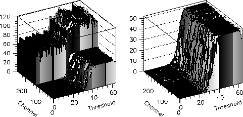
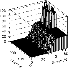
HDIs H1-13 and H1-29. There are chips on both HDIs which have several channels that sometime fire even when masked OFF. The firing rate is typically not 100%. The channels on a given chip tend to come on together, i.e. some events have all channels OFF (as they should) and some events have a large number of channels ON. The time stamp on these events is random. The TOT is mostly 1 or 15. This kind of problem was also seen in some chips on the testbeam module (rad soft V1). Note that on the testbeam module this problem was intermittent, i.e. there were intervals of several hours were the problem disappeared. As discussed below, we have reasons to believe that this kind of problem can still be intermittent. If this is indeed the case, we will have a hard time eliminating all the chips with this problem at an early stage in the testing process.:
HDI H1-29 (DFA D02F-4), chip 13. Read back tests of control registers and masks stopped working. The read back bits were typically the same as the written bits, but shifted by one position within the word.
With 60% duty cycle, the read back tests of the masks on chip 13 worked. The read back tests of the control registers did not work.
With 40% duty cycle, the read back tests of the control registers on chip 13 worked. The read back tests of the masks did not work.
With 60% duty cycle, the data from chip 12 was not valid. Normally an event from a given chip consists of two bytes of header, two bytes per hit, and two empty trailer bytes. Hence, depending on the number of hits, the first trailer byte must be the 3rd or 5th or 7th.... byte of data from a given chip. The first trailer byte for chip 12 was always found at an even position in the byte sequence.
![]()