Gain / Intercept
Measurement
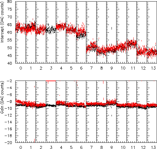
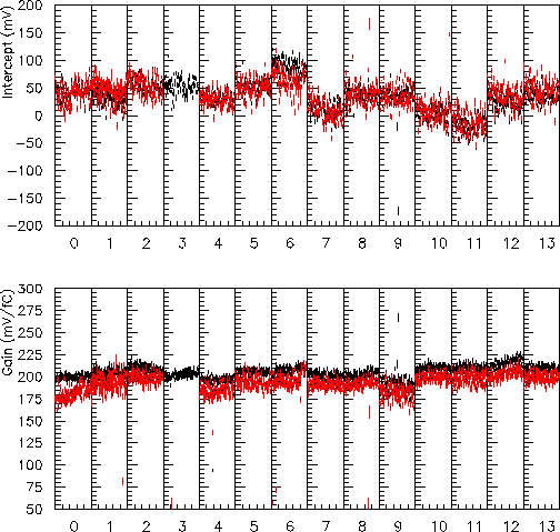
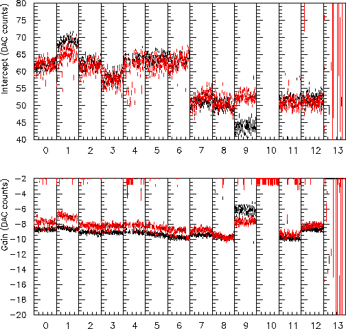
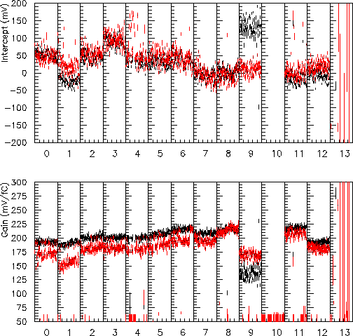
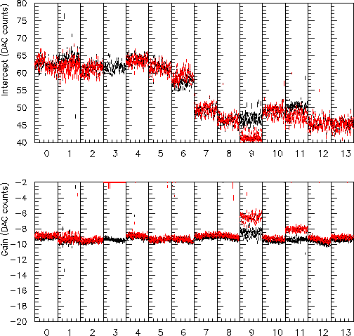
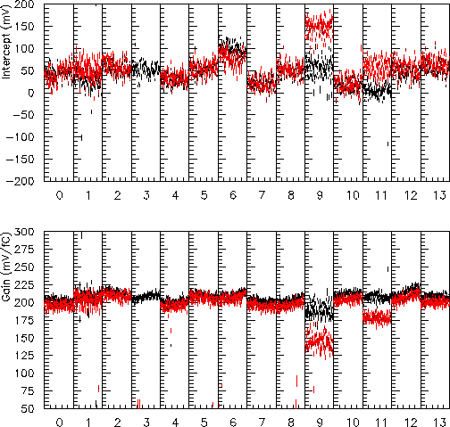
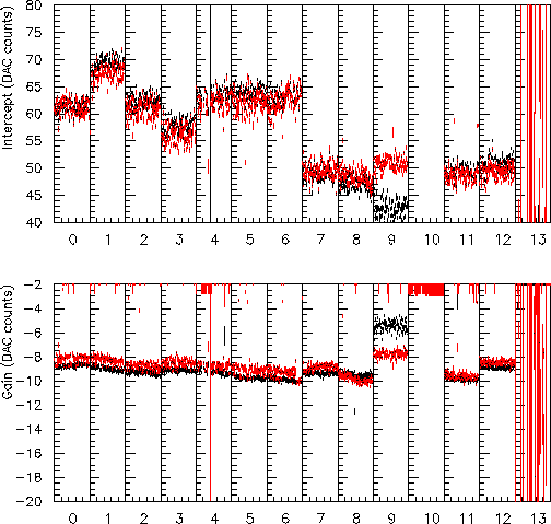
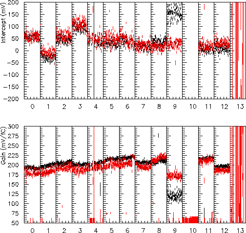
The results of the gain and intercept measurements for all channels are
summarized in the plots below. The results are presented in units of
DAC counts and in SI units. The chip numbers are also shown.
The data before bonding to the silicon are in black.
The data after bonding to the silicon are in red.


Gains and intercepts for H1-13 (D02B-8) at 100 nsec shaping time.
A ps file with many more plots is
also available.


Gains and intercepts for H1-29 (D02F-4) at 100 nsec shaping time.
A ps file with many more plots is
also available.


Gains and intercepts for H1-13 (D02B-8) at 400 nsec shaping time.
A ps file with many more plots is
also available.


Gains and intercepts for H1-29 (D02F-4) at 400 nsec shaping time.
A ps file with many more plots is
also available.
Tables of the gain and offset measurements can be found
here .
Some observations:
- The gains before bonding to the silicon are of order of 200 mV/fC.
- The gains after bonding to the silicon drop by as much as 10% on the n (phi) side
and 6% on the p (z) side.
- The gains measured with a 400 ns shaping time are typically higher
than the gains measured with a 100 ns shaping time by 2 to 5 %.
- At the request of chip experts, we also measured the gains at 200 nsec,
where the differences between bonded and unbonded channels are
expected to be smaller. We did this, after bonding, for chip 6
of HDI H1-13 (DFA D02B-8).
This chip is
the last chip on the n-side. The last few channels on this
chip are not bonded, and this provides a convenient way of
comparing gains for bonded and unbonded channels. The results
of this study are available
here.
The upshot is that the gain for a shaping time of 200 nsec is of
order 250 mV/fC, and bonded channels show a drop in gain of
7.5%.
- The offset (intercept) dispersion on a given chip
typically has an RMS of order 13 mV before bonding to the silicon
and 16 mV after bonding to the silicon.
- The intercepts in DAC counts are defined as the extrapolated threshold
for CAL_DAC = 0 on the n-side and CAL_DAC = 63 on the p-side. According
to our understanding of the average chip parameters,
this corresponds to 0.0 fC injected charge on the
n-side and 0.8 fC on the p-side. This is why the intercepts in DAC counts
are systematically different on the two sides.
The intercepts in mV are defined at nominal zero injected charge, and
they are much more uniform.
- The gain of chip 9 on both
the forward and backward HDI is strange,
as can be seen from the distributions above. In addition,
the
noise measurements for chip 9 show a component of
coherent noise bursts that is not present on other chips.
Similar but smaller effects on chip 9 were also seen in the tests of
the first H1 hybrid of new design loaded with rad hard V1 chips.
This may be an unlikely coincidence
or a problem with the UCSB test stand that affects chip 9 strongly.
This is unlikely, because the hybrids were tested in two very
different configurations, first in the ringframe and then in the
commissioning box, and the behavior of chip 9 was consistent between
the two setups.
A problem with the HDI layout is also unlikely since chip 9 is not in the
same physical location on a forward and a backward HDI, however there
may be second order effects which cause the chip at this location
on the p-side to be more sensitive to HDI problems (????)

Back to contents...
Forward to the next section...
