First results from commissioning at IR2 have cast doubts on
our ability to measure the offsets on the AToM chip.
A study of occupancy seems to suggest that the offsets determined
from threshold scans at different charge injection values are not
the real offsets for the chips. (A description of the offset-determination
procedure, which does not include the corrections discussed below,
is available here).
It has been suggested by several people that chip-to-chip variations
in the properties of the CAL DAC may introduce large systematic
uncertainties in our offset determination. Basically this is
due to the fact that offsets in the CAL DAC result in a finite amount
of charge being injected even when the digital value of the CAL DAC
is set at zero.
Indeed, using
test data from
Honeywell, one can calculate that the offsets obtained in
the usual way should be corrected on average by 3.0 THR DAC
counts on the n-side and 12.4 THR DAC counts on the p-side.
Furthermore, these corrections have an RMS spread of 2.0 THR DAC
counts on the n-side and 2.9 THR DAC counts on the p-side.
It should be pointed out that for the commissioning module no
correction was applied to the offsets on the n-side, while on
the p-side the offsets were corrected by about 14 counts.
To set the scale, 1 THR DAC count corresponds to a charge of
order 330 electrons; the noise for a layer 2 detector is of order
3-4 THR DAC counts; the RMS spread on the offset for channels on
a given chip is of order 1.5 THR DAC counts.
The obvious question is whether the data from the tests at Honeywell
can be used to apply a chip dependent corrections to the offsets.
Unfortunately no such data are available for the chips mounted on
the commissioning module. We have therefore used hybrid H1-18
(unbonded) in an attempt to address this issue. All measurements
reported here are at 100 nsec peaking time, and with a 40 MHZ clock.
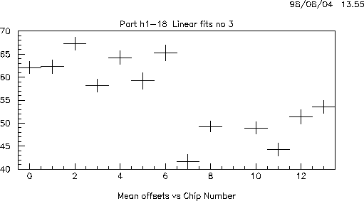
In Figure 1, we show the uncorrected mean offset as a function of chip number.
Chips 0-6 are on the n-side, chips 7-13 are on the p-side. The error
bars reflect the rms channel-to-channel spread, not the error in the
mean (which is about 10 times smaller). Note the expected systematic
difference between the n and p sides.
Figure 1: Uncorrected mean offset as a function of chip number
determined
from threshold scans at different charge injections.
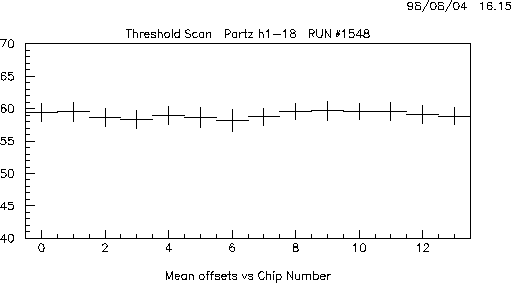
As a measure of the chip-to-chip spread in the offsets, we took a high
statistics threshold scan run with no charge injection (i.e. just
looking at noise hits). Then we extracted for each
channel the threshold that gives an occupancy of 50%. Note that this
is not the real offset. It corresponds to the threshold
at which there is a 50% probability of finding a 0 to 1 transition
of the comparator within the trigger jitter window
(3 microseconds in our case).
However, this 50% point (P50) is related to the real offset (O)
by something like:
P50 = O + f(noise)
where f(noise) is an (unknown) function of the noise. (In principle
one might be able to calculate f(noise), but the reliability
of such a calculation may be questionable...).
Since in our case
the noise is the same for all channels, f(noise) is just a constant and
P50 is a good measure of the
relative offset. The average P50 as a function of chip number is
shown in Figure 2; the error bars are the RMS channel-to-channel
spread.
Figure 2: Mean threshold for 50% noise occupancy as a function of
chip number.
The distribution in Figure 2 strongly suggests that the chip-to-chip
spread in real offsets is much smaller than in Figure 1, even accounting
for the expected differences between n and p sides. We believe
that offsets corrected only in a global way are effectively meaningless.
This explains, at least qualitatively, the IR2 observations.
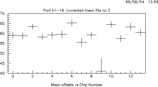
The next step of course is to correct the offsets from Figure 1 using
Honeywell data. This is shown in Figure 3 (again, error bars are channel-
to-channel spreads). The correction is performed using the measured
analog properties of the calibration DAC as a function of chip number,
as well as the measured gain in counts as a function of chip and
channel number (the gain is used to extrapolate the offset measurements
to true zero charge injection).
Figure 3:Mean offset as a function of chip number
determined
from threshold scans at different charge injections and corrected
using Honeywell data.
The spread in chip-to-chip offsets in Figure 3 is somewhat smaller
than in Figure 1, but is still significantly larger than the P50
spread in Figure 2. Therefore we conclude that we cannot reliably
use the Honeywell data to correct the offset measurements.
It is also not clear whether
threshold scans at different charge injections could be used to monitor
time-dependent offset shifts, since with this method
there is no way to distinguish shifts in amplifier offsets from
shifts in CAL DAC offsets (for example). On the other hand,
occupancy measurements such as the one shown in Figure 2 could
in priciple be used at IR2 to monitor such shifts.
However, this method is complicated by its noise dependence (recall
in our notation P50 = O + f(noise)).
We are now investigating the possibility of extracting offsets without
using the charge injection circuitry. The sparsification algorithm
adopted by the AToM chip designers complicates the issue somewhat
(well, actually, a lot !). We have some ideas that we are pursuing.